

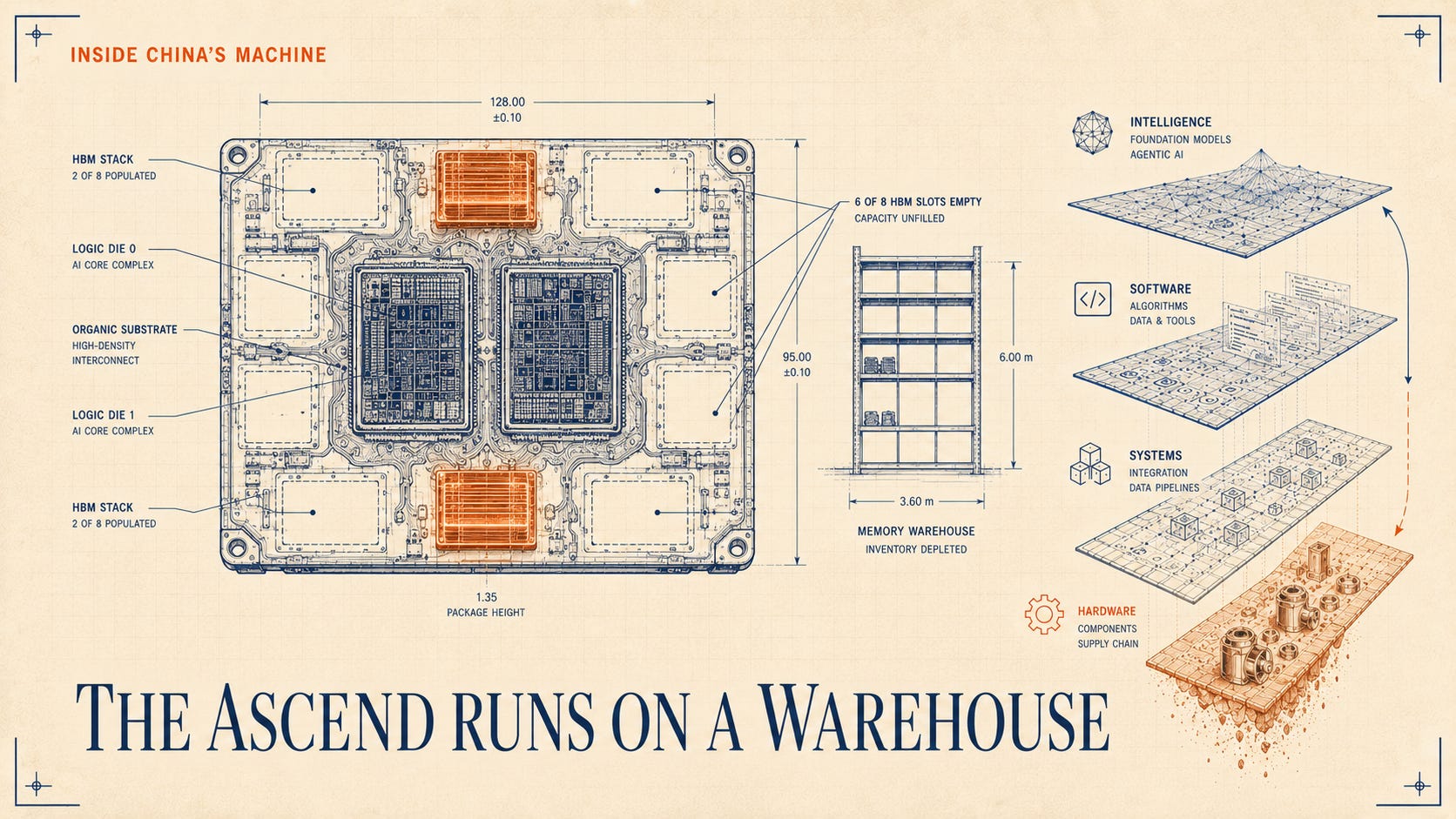
Take apart an Ascend 910C, Huawei’s flagship AI accelerator, and you find something the press releases do not mention.
TechInsights did exactly that, and their teardown reports logic dies fabricated by TSMC in 2020, sitting alongside HBM2E memory stacks from Samsung and SK Hynix. Chinese trade coverage of the same chip has repeatedly described its localization rate as exceeding 90 percent.
The press release and the X-ray disagree. That gap is where this issue lives, because it points at the thing almost every analysis of China’s AI compute position gets wrong: the chokepoint is not where the export controls aimed it.
Everyone is watching the wrong layer
The public conversation about Chinese AI silicon runs on lithography. EUV machines, ASML, SMIC’s 7-nanometer process, the question of whether China can reach 5. It is a coherent story and it produces a clear scoreboard, which is probably why it dominates.
It is also, at this moment, not the binding constraint.
SemiAnalysis, working from supply-chain data, puts the position bluntly: China could easily build more than 805,000 Ascend accelerators in a year from available TSMC and SMIC capacity, but it will not, because it does not have enough HBM. The wafers are not the problem. The logic dies are not the problem. China has fab capacity it cannot convert into accelerators, because it lacks the memory to package next to the compute.
This deserves to sit for a moment, because it inverts the entire framing of the export-control debate. The controls were designed around the assumption that if you deny a country the ability to print advanced logic, you deny it advanced compute. China’s answer was to route around lithography with chiplets, older nodes, and brute force. That answer worked, in the narrow sense that the dies exist. And it ran straight into a wall nobody was pointing at, which is that an AI accelerator is not a logic die. It is a logic die surrounded by high-bandwidth memory, and the memory is the part China cannot yet make at scale.
The workaround for one bottleneck created another
Look at how the 910C is actually built, because the engineering tells you the cost of the detour.
Unable to print a large monolithic die at an advanced node, Huawei took two 910B dies and packaged them together, each on its own interposer, connected through an organic substrate. This is a legitimate strategy. It is cheaper, it yields better, and it ramps faster than the advanced packaging Nvidia uses.
It also has a price, and the price is bandwidth. Independent analysis suggests the die-to-die bandwidth of this arrangement runs an order of magnitude or more below Nvidia’s packaging, and the chip-to-chip interconnect sits around 400 GB/s, well under half of what NVLink provides. For workloads dominated by all-reduce communication, which is to say large-scale distributed training, that is precisely the wrong place to be slow.
So the substitution chain runs like this. Denied advanced lithography, China substitutes chiplets. Chiplets require advanced packaging to preserve bandwidth. Advanced packaging is also restricted. The result is a chip whose compute is respectable and whose ability to talk to itself, and to its neighbors, is not.
Reported memory bandwidth figures for the 910C vary across sources by nearly a factor of two, which is itself worth noting: this is a domain where confident numbers should be treated with suspicion. But every source, including the favorable ones, places it below the H100. The compute gap is manageable. The memory and interconnect gap is the one that decides what can actually be trained.
Huawei is running on inventory, and inventory has a maturity date
Here is the fact that turns a technical observation into a capital judgment.
Before the export controls on high-bandwidth memory took effect, Chinese buyers acquired a large stockpile of HBM stacks. SemiAnalysis, again from supply-chain reconstruction rather than any disclosure, puts it at roughly 13 million. An Ascend 910C carries eight. That stockpile is therefore sufficient to package on the order of 1.6 million accelerators, which is a large number and which is also, precisely, a finite one.
Treat the figure as an estimate, because it is one, and no Chinese entity has published it. But the shape of the claim does not depend on the precision of the number. Whatever the exact count, it was bought once, it is being drawn down, and nobody is selling more.
The same is true of the logic. TechInsights found TSMC dies from 2020 inside a 2025-era chip, and SemiAnalysis estimates that this die bank depletes within months rather than years.
Huawei’s AI accelerator business is currently running on a warehouse. That is not a criticism of Huawei, which stockpiled intelligently and under duress, and it is not a prediction of collapse. It is a statement about what kind of asset the current production run represents. Capability compounds. Inventory depletes. The two look identical on a shipment chart and they are not remotely the same thing, and anyone reading Ascend volumes as evidence of a structural position is reading an inventory drawdown as if it were a capacity curve.
Which means the entire question becomes: what replaces the warehouse?
The company that decides this is not the company everyone is watching
The answer is CXMT, ChangXin Memory Technologies, and it is one of the most remarkable industrial stories in China right now, for reasons that have almost nothing to do with AI.
CXMT is winning, spectacularly, in conventional DRAM. One caveat has to come first, and it matters more than it looks: CXMT is private and pre-IPO, so none of its financials are audited public filings. Every figure below is a reported number, and the reporting traces back largely to a single analysis house. Hold them accordingly.
With that said, the reported figures are extraordinary. First quarter 2026 revenue of about 50.8 billion yuan, up more than 700 percent year on year. Net profit around 33 billion. Margins near 70 percent, which would place it in the same band as SK Hynix. A first annual profit in 2025. SemiAnalysis expects its wafer capacity to approach Micron’s by the end of 2026, at roughly 350,000 wafers per month against Micron’s 385,000. Omdia has its global DRAM revenue share rising from under 4 percent in mid-2025 to around 8 percent. From a standing start a decade ago, this is one of the great catch-up performances in semiconductor history, and it should be described as one.
But read the margin honestly, because the company’s defenders and its critics both misread it. SemiAnalysis finds CXMT’s DDR5 cost per bit still runs more than 30 percent above the big three. The 70 percent margin is not a cost victory or a technology victory. It is a price. DRAM prices exploded, and CXMT is holding a lot of DRAM.
None of that gates AI compute.
Conventional DRAM is not HBM. HBM is DRAM stacked vertically and connected with through-silicon vias, and the stacking is the hard part. And in HBM, the picture is entirely different.
At the end of 2025, SemiAnalysis puts CXMT’s HBM allocation at roughly 5,000 wafers per month out of about 265,000 wafers of total capacity. Under two percent. The same analysis has CXMT still struggling to stabilize production of 8-high HBM3, with 12-high harder still, and industry estimates put the 8-high yield near 25 percent. Roughly 99 percent of CXMT’s 2025 bit shipments were conventional DDR and LPDDR.
None of that is a scandal. It is a rational allocation, and the reason is the most important sentence in this issue.
Bulk DRAM currently carries better margins than CXMT’s HBM, and it produces more than three times the bits from the same wafer area. For a company optimizing its own economics, every wafer moved to HBM is a wafer earning less. The commercially correct decision and the nationally required decision point in opposite directions, and the company is currently making the commercially correct one.
Which brings us to the document that settles the argument.
The use of proceeds is the company telling you what it will actually do
CXMT opens IPO subscription on July 16, raising 29.5 billion yuan on the STAR Market. It is the largest A-share listing of 2026 and the second-largest in STAR Market history, behind SMIC’s 53.2 billion yuan offering in 2020.
Read where the money goes. Roughly 69.5 percent of net proceeds funds wafer production lines and DRAM technology upgrades. The remaining 30.5 percent funds forward-looking DRAM research. There is no dedicated HBM project and no separate HBM line in the use of proceeds, an absence noted independently by SemiAnalysis, by the Seoul Economic Daily, and in Korean industry coverage of the filing.
This is worth stating carefully, because it is the load-bearing claim of the issue. The prospectus is not silent about HBM as a subject; a filing of that size discusses its technology roadmap and its risks. What it does not contain is money earmarked for it. And a use of proceeds is not a press release. It is a legal commitment about where four billion dollars will go, and it goes to commodity memory.
So the schedule the market is pricing, in which CXMT ramps HBM and relieves the constraint on Chinese AI compute, is not the schedule the company has just funded.
What this does to a valuation, and to our own prior work
At the indicated offering price, CXMT lists at a market capitalization near 295 billion yuan. That is not the number worth looking at. Chinese market commentary is discussing a theoretical post-listing valuation of two to three trillion yuan.
Sit with the upper end of that. The largest company on the entire A-share market today is China Construction Bank, at roughly 2.63 trillion yuan. The number being floated for a memory manufacturer would make it the most valuable listed company in China.
Read the two halves of the business separately, which is the discipline this publication keeps arriving at. The conventional DRAM franchise is genuine, profitable, and world-class, and it is enjoying a historic price cycle. On its own it justifies a large number. But it is a cyclical commodity business whose current margin comes from scarcity rather than from cost advantage, and it is being valued as though the cycle were a moat. The HBM business, meanwhile, is the strategic asset of enormous national importance, and it is the one the company has just declined to fund.
Those two things are being sold as one company, and at IPO they will be discounted at one rate.
The number to watch is not SMIC’s next node announcement, which will be covered everywhere. It is CXMT’s HBM wafer allocation and its 8-high stacking yield, which will be covered almost nowhere. That is what decides how many accelerators China can build once the warehouse is empty, and therefore how much compute the entire Chinese AI industry has to work with.
There is a consequence for our own argument too, and it needs stating.
Two issues ago we argued that the binding constraint on embodied AI is data rather than compute, on the grounds that GPU clusters capable of training vision-language-action models are commercially available. That was accurate then and it is accurate now. What this issue adds is a maturity date on it. Compute has been available in China because of a stockpile bought before a door closed. If CXMT’s HBM ramp slips and the warehouse empties, compute stops being the abundant input and becomes a contested one, and the data argument, while still correct on its own terms, stops being the only thing that matters.
A constraint that is currently non-binding is not the same as a constraint that has been solved. The data thesis holds. It now holds conditionally, and the condition has a name, and the name is a yield rate in Hefei.
Read the seam between the memory and the model
Silicon is the substrate. Models are the intelligence that runs on it. The seam between those two layers is not measured in nanometers, and it is not measured in floating-point operations either. It is measured in how fast you can move a parameter from memory into a multiplier, and how fast two chips can agree on a gradient.
That is why the chokepoint moved without anyone noticing. Everyone was watching the layer that gets photographed, the fab, the machine, the node. The constraint quietly relocated to the layer that gets soldered next to it.
China’s AI compute ceiling in 2027 will not be set by a lithography breakthrough. It will be set by two things happening inside one company in Hefei: whether it can push its DRAM core die to a competitive node without EUV, and whether it can stack eight of those dies reliably, at volume, in the back end. The first is a process problem. The second is a packaging problem. Neither is what the export controls were designed around, and neither is what the market is watching.
And there is a third thing, which is not an engineering problem at all. It is whether the company chooses to. This week, with four billion dollars in hand, it chose commodity DRAM.
Inside China’s Machine is research, not investment advice. The 910C teardown findings are Confirmed from TechInsights. The IPO size, subscription date, and the allocation of net proceeds are Confirmed from CXMT’s prospectus and the exchange filings as reported by Caixin, the South China Morning Post, and Reuters. The absence of a dedicated HBM line in the use of proceeds is reported independently by SemiAnalysis and by Korean industry coverage including the Seoul Economic Daily; readers should note that some generalist outlets have characterized the proceeds as funding an HBM push, and the two readings are in tension. Ascend production capacity, HBM stockpile volumes, die-bank depletion timing, CXMT’s HBM wafer allocation, and its DDR5 cost position are Estimated and attributed to SemiAnalysis, whose supply-chain figures are reconstructions rather than primary filings. The 8-high HBM3 yield figure is an industry estimate. The two to three trillion yuan figure is market commentary, not a forecast by this publication, and is cited as evidence of what is being priced rather than as a valuation. Reported memory bandwidth figures for the 910C conflict across sources and are treated accordingly in the text. Current as of July 12, 2026.